
Total Reflection Mirrors: Nanostructures for X-ray Optics
Two silicon substrates are refined with state-of-the-art thin-film coatings for free-electron laser applications at the Deutsches Elektronen Synchrotron (DESY). Nanotechnologists from Geesthacht manufacture ultra-high precision X-ray optics for FLASH II required for this process.
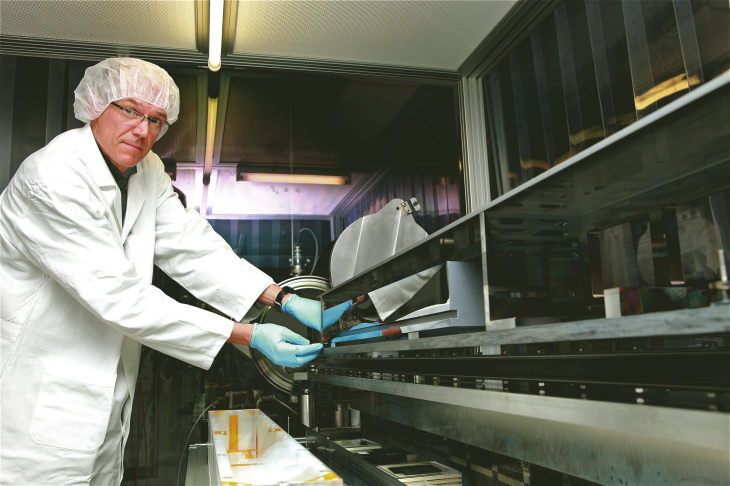
After the refining process: Dr. Michael Störmer removes the new X-ray mirror from the coating facility. Photo: HZG/Torsten Fischer
Scientists around the world make use of many different forms of X-ray light in their experiments, as this light simply passes through most materials. Researchers can thus create X-ray images of single molecules or atomic processes. For the beam to be utilized, it has to be directed to the experimental stations. However, how can a beam, which passes through virtually everything, be redirected?
The answer is provided by high precision mirrors which are refined with high-tech coating layers at the Helmholtz Zentrum Geesthacht.
Scientists at the Department of Nanotechnology have developed a coating facility in which silicon substrates, of almost one metre in length and 12 kilograms in weight, are refined with three ultrathin layersside-by-side. The worldwide unique two X-ray mirrors, were recently produced for beam guidance in the free-electron laser FLASH II at the DESY in Hamburg.
No tolerance for deviations
The technical requirements of the X-ray mirrors were extreme: a deviation in layer thickness of less than 2 nanometres is acceptable at a total film thickness of 35 nanometres and along a whole mirror length of 82 centimetres. Converted, this would mean that an approx. 90 kilometre stretch of railway track from Hamburg to Kiel might only deviate by 0.2 millimetres on its entire length.
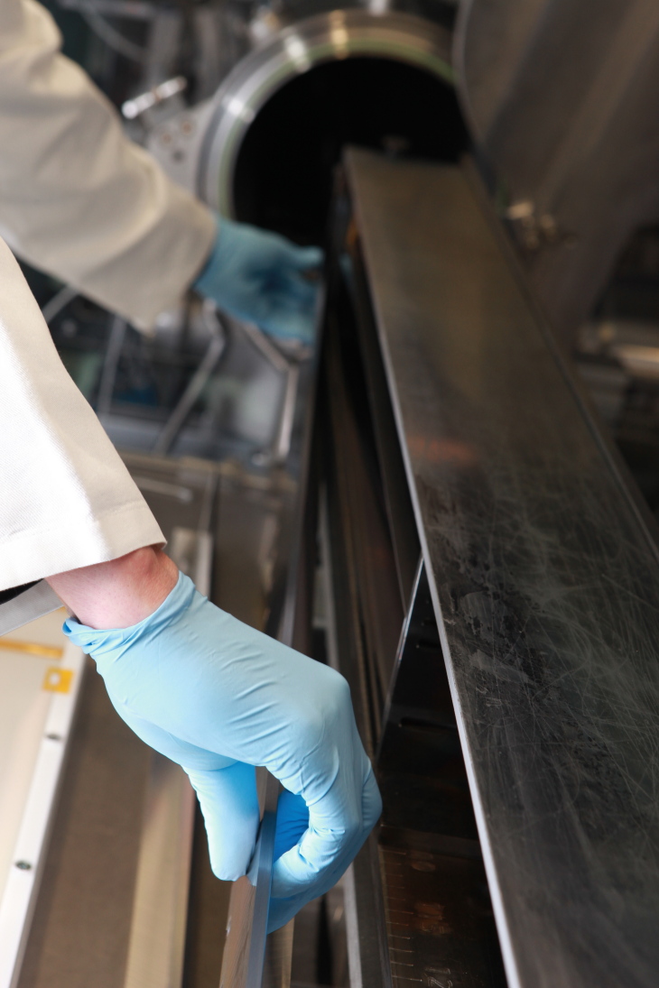
Three layers were sputtered onto a silicon substrate: This is utilised to reflect X-ray beams in the FLASH II facility. Photo: HZG/Torsten Fischer
Not only one, but three uniform layers, had to be applied next to each other along the 82 centimetres length. The HZG scientist, Dr. Michael Störmer, who developed the coating facility, explained: “Only very few groups in the entire world are in a position to achieve this. The layers and the mirrors have practically no tolerance and must be absolutely flat along the entire length of the mirror, as the X-ray light beams always spread out in a parallel and linear manner“.
This alignment of the photons must be maintained when the light is redirected by means of a mirror. If the surface of the mirror is not perfectly smooth, the reflection of the light waves is distorted and the desired properties of the X-ray laser light are lost.
For the FLASH II applications, the first layer is made of nickel, the second layer is amorphous carbon and the third layer is the very temperature stable substance boron carbide. The material properties of the layers thus contribute to the ability of the mirror to transport the high intensity of the short X-ray flashes.
The layers are applied in an argon vacuum in the facility, using plasma sputtering technology. Sputtering is a physical process whereby atoms are ejected from a solid body (target), due to bombardment of the target with high energy ions (primarily noble gas ions), and enter into the plasma (from Wikipedia).
These atoms are ejected e.g. from a nickel, boron carbide or carbon target, spread out and form a fine layer on the opposite silicon substrate. The atoms condense to a firm film on the substrate and the unique coating is accomplished.
More Information:
Department NanotechnologyContact

Helmholtz-Zentrum Geesthacht - Zentrum für Material- und Küstenforschung
Phone: +49 (0)4152 87-1648
E-mail contactMax-Planck-Straße 1
21502 Geesthacht